Readings Newsletter
Become a Readings Member to make your shopping experience even easier.
Sign in or sign up for free!
You’re not far away from qualifying for FREE standard shipping within Australia
You’ve qualified for FREE standard shipping within Australia
The cart is loading…


This title is printed to order. This book may have been self-published. If so, we cannot guarantee the quality of the content. In the main most books will have gone through the editing process however some may not. We therefore suggest that you be aware of this before ordering this book. If in doubt check either the author or publisher’s details as we are unable to accept any returns unless they are faulty. Please contact us if you have any questions.
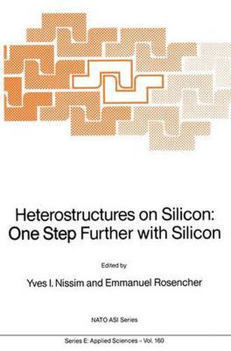
In the field of logic circuits in microelectronics, the leadership of silicon is now strongly established due to the achievement of its technology. Near unity yield of one million transistor chips on very large wafers (6 inches today, 8 inches tomorrow) are currently accomplished in industry. The superiority of silicon over other material can be summarized as follow: - The Si/Si0 interface is the most perfect passivating interface ever 2 obtained (less than 10 e y-I cm2 interface state density) - Silicon has a large thermal conductivity so that large crystals can be pulled. - Silicon is a hard material so that large wafers can be handled safely. - Silicon is thermally stable up to 1100 DegreesC so that numerous metallurgical operations (oxydation, diffusion, annealing … ) can be achieved safely. - There is profusion of silicon on earth so that the base silicon wafer is cheap. Unfortunatly, there are fundamental limits that cannot be overcome in silicon due to material properties: laser action, infra-red detection, high mobility for instance. The development of new technologies of deposition and growth has opened new possibilities for silicon based structures. The well known properties of silicon can now be extended and properly used in mixed structures for areas such as opto-electronics, high-speed devices. This has been pioneered by the integration of a GaAs light emitting diode on a silicon based structure by an MIT group in 1985.
$9.00 standard shipping within Australia
FREE standard shipping within Australia for orders over $100.00
Express & International shipping calculated at checkout
This title is printed to order. This book may have been self-published. If so, we cannot guarantee the quality of the content. In the main most books will have gone through the editing process however some may not. We therefore suggest that you be aware of this before ordering this book. If in doubt check either the author or publisher’s details as we are unable to accept any returns unless they are faulty. Please contact us if you have any questions.
In the field of logic circuits in microelectronics, the leadership of silicon is now strongly established due to the achievement of its technology. Near unity yield of one million transistor chips on very large wafers (6 inches today, 8 inches tomorrow) are currently accomplished in industry. The superiority of silicon over other material can be summarized as follow: - The Si/Si0 interface is the most perfect passivating interface ever 2 obtained (less than 10 e y-I cm2 interface state density) - Silicon has a large thermal conductivity so that large crystals can be pulled. - Silicon is a hard material so that large wafers can be handled safely. - Silicon is thermally stable up to 1100 DegreesC so that numerous metallurgical operations (oxydation, diffusion, annealing … ) can be achieved safely. - There is profusion of silicon on earth so that the base silicon wafer is cheap. Unfortunatly, there are fundamental limits that cannot be overcome in silicon due to material properties: laser action, infra-red detection, high mobility for instance. The development of new technologies of deposition and growth has opened new possibilities for silicon based structures. The well known properties of silicon can now be extended and properly used in mixed structures for areas such as opto-electronics, high-speed devices. This has been pioneered by the integration of a GaAs light emitting diode on a silicon based structure by an MIT group in 1985.