Readings Newsletter
Become a Readings Member to make your shopping experience even easier.
Sign in or sign up for free!
You’re not far away from qualifying for FREE standard shipping within Australia
You’ve qualified for FREE standard shipping within Australia
The cart is loading…


This title is printed to order. This book may have been self-published. If so, we cannot guarantee the quality of the content. In the main most books will have gone through the editing process however some may not. We therefore suggest that you be aware of this before ordering this book. If in doubt check either the author or publisher’s details as we are unable to accept any returns unless they are faulty. Please contact us if you have any questions.
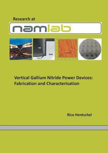
Efficient power conversion is essential to face the continuously increasing energy consumption of our society. GaN based vertical power field effect transistors provide excellent performance figures for power-conversion switches, due to their capability of handling high voltages and current densities with very low area consumption. This work focuses on a vertical trench gate metal oxide semiconductor field effect transistor (MOSFET) with conceptional advantages in a device fabrication preceded GaN epitaxy and enhancement mode characteristics. The functional layer stack comprises from the bottom an n+/n–drift/p-body/n+-source GaN layer sequence. Special attention is paid to the Mg doping of the p-GaN body layer, which is a complex topic by itself. Hydrogen passivation of magnesium plays an essential role, since only the active (hydrogen-free) Mg concentration determines the threshold voltage of the MOSFET and the blocking capability of the body diode. Fabrication specific challenges of the concept are related to the complex integration, formation of ohmic contacts to the functional layers, the specific implementation and processing scheme of the gate trench module and the lateral edge termination. The maximum electric field, which was achieved in the pn- junction of the body diode of the MOSFET is estimated to be around 2.1 MV/cm. From double-sweep transfer measurements with relatively small hysteresis, steep subthreshold slope and a threshold voltage of 3 - 4 V a reasonably good Al2O3/GaN interface quality is indicated. In the conductive state a channel mobility of around 80 - 100 cm(2)/Vs is estimated. This value is comparable to device with additional overgrowth of the channel. Further enhancement of the OFF-state and ON-state characteristics is expected for optimization of the device termination and the high-k/GaN interface of the vertical trench gate, respectively. From the obtained results and dependencies key figures of an area efficient and competitive device
$9.00 standard shipping within Australia
FREE standard shipping within Australia for orders over $100.00
Express & International shipping calculated at checkout
This title is printed to order. This book may have been self-published. If so, we cannot guarantee the quality of the content. In the main most books will have gone through the editing process however some may not. We therefore suggest that you be aware of this before ordering this book. If in doubt check either the author or publisher’s details as we are unable to accept any returns unless they are faulty. Please contact us if you have any questions.
Efficient power conversion is essential to face the continuously increasing energy consumption of our society. GaN based vertical power field effect transistors provide excellent performance figures for power-conversion switches, due to their capability of handling high voltages and current densities with very low area consumption. This work focuses on a vertical trench gate metal oxide semiconductor field effect transistor (MOSFET) with conceptional advantages in a device fabrication preceded GaN epitaxy and enhancement mode characteristics. The functional layer stack comprises from the bottom an n+/n–drift/p-body/n+-source GaN layer sequence. Special attention is paid to the Mg doping of the p-GaN body layer, which is a complex topic by itself. Hydrogen passivation of magnesium plays an essential role, since only the active (hydrogen-free) Mg concentration determines the threshold voltage of the MOSFET and the blocking capability of the body diode. Fabrication specific challenges of the concept are related to the complex integration, formation of ohmic contacts to the functional layers, the specific implementation and processing scheme of the gate trench module and the lateral edge termination. The maximum electric field, which was achieved in the pn- junction of the body diode of the MOSFET is estimated to be around 2.1 MV/cm. From double-sweep transfer measurements with relatively small hysteresis, steep subthreshold slope and a threshold voltage of 3 - 4 V a reasonably good Al2O3/GaN interface quality is indicated. In the conductive state a channel mobility of around 80 - 100 cm(2)/Vs is estimated. This value is comparable to device with additional overgrowth of the channel. Further enhancement of the OFF-state and ON-state characteristics is expected for optimization of the device termination and the high-k/GaN interface of the vertical trench gate, respectively. From the obtained results and dependencies key figures of an area efficient and competitive device
Search our extensive online catalogue.
