Readings Newsletter
Become a Readings Member to make your shopping experience even easier.
Sign in or sign up for free!
You’re not far away from qualifying for FREE standard shipping within Australia
You’ve qualified for FREE standard shipping within Australia
The cart is loading…


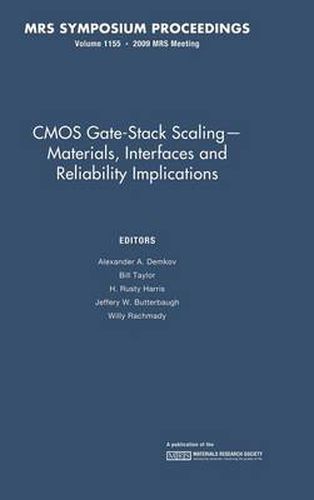
To address the increasing demands of device scaling, new materials are being introduced into conventional Si CMOS processing at an unprecedented rate. Presentations collected here focus on understanding, from a chemistry and materials perspective, the mechanism of interface formation and defects at interfaces, for both conventional Si and alternative channel (Ge or III-V) systems. Several papers address reliability concerns for high-k/metal gate (basic physical models, charge trapping, etc.), while others cover characterization of the thin films and interfaces which comprise the gate stack. Topics include: advanced Si-based gate stacks; and alternate channel materials.
$9.00 standard shipping within Australia
FREE standard shipping within Australia for orders over $100.00
Express & International shipping calculated at checkout
To address the increasing demands of device scaling, new materials are being introduced into conventional Si CMOS processing at an unprecedented rate. Presentations collected here focus on understanding, from a chemistry and materials perspective, the mechanism of interface formation and defects at interfaces, for both conventional Si and alternative channel (Ge or III-V) systems. Several papers address reliability concerns for high-k/metal gate (basic physical models, charge trapping, etc.), while others cover characterization of the thin films and interfaces which comprise the gate stack. Topics include: advanced Si-based gate stacks; and alternate channel materials.