Readings Newsletter
Become a Readings Member to make your shopping experience even easier.
Sign in or sign up for free!
You’re not far away from qualifying for FREE standard shipping within Australia
You’ve qualified for FREE standard shipping within Australia
The cart is loading…


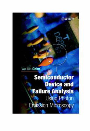
The diminishing size and greater complexity of modern semiconductor integrated circuits poses new challenges in fault detection. Photon Emission Microscopy (PEM) is a physical fault localisation technique used for analysing IC failures. Detailing the PEM technique and its application to semiconductor device analysis, this unique reference:
* Illustrates the application of the PEM technique in various areas of device reliability, in particular hot-carrier, oxide and ESD reliability.
* Presents the principles of design and calibration for a spectroscopic emission microscope system along with coverage of the three main operation modes: frontside, backside and spectroscopic PEM
* Provides an analysis of light emission in semiconductors under hot-carrier and high-field impulse stressing in MOS transistors and photon emission from biased MOS capacitors.
Not only an essential reference for researchers and students in the field, the numerous practical examples throughout the text also make this an indispensible guide for failure analysis engineers and microelectrics industry professionals.
$9.00 standard shipping within Australia
FREE standard shipping within Australia for orders over $100.00
Express & International shipping calculated at checkout
The diminishing size and greater complexity of modern semiconductor integrated circuits poses new challenges in fault detection. Photon Emission Microscopy (PEM) is a physical fault localisation technique used for analysing IC failures. Detailing the PEM technique and its application to semiconductor device analysis, this unique reference:
* Illustrates the application of the PEM technique in various areas of device reliability, in particular hot-carrier, oxide and ESD reliability.
* Presents the principles of design and calibration for a spectroscopic emission microscope system along with coverage of the three main operation modes: frontside, backside and spectroscopic PEM
* Provides an analysis of light emission in semiconductors under hot-carrier and high-field impulse stressing in MOS transistors and photon emission from biased MOS capacitors.
Not only an essential reference for researchers and students in the field, the numerous practical examples throughout the text also make this an indispensible guide for failure analysis engineers and microelectrics industry professionals.